
GameBoyã
General Purpose Interface
Designers Manual
By S.G.Willis Rev 1.1
1.0 Introduction
The GameBoy general purpose
interface 'GBGPI' converts a GBpocket or GBcolour into a multipurpose
programmable development platform. The software defined input and output ports
interface enables connection to a wide variety of sensor and control devices.
Making GBGPI ideal for robotics, home control or portable development projects.
The dual boot internal flash
ROM allows you to develop and simulate programs on your PC, then download them
via the game link port to the GBGPI cartridge, eliminating the need for a
dedicated programmer. Once programmed simply flip the boot switch and your
ready to go!
A library of interface
modules are provided, these can be added to the 'C' compiler - GBDK allowing
connection to analogue, logic, thermistor, RTC and many more sensor
devices. The use of a high level
development language makes programming easier to understand and readable to
others.
1.1 Key Features:
12 Channel 8bit High
Speed ADC
8 Channel 8bit Buffered DAC
32KB of Internal Flash Program ROM
4KB of Internal Flash Data Store
Dual Boot Mode for Reprogramming
No Programmer Required
Rail-to-Rail Inputs and Outputs (0 to 5V)
Standard D25 Output Connector
6hrs Operation from NiMH Batteries
'C' Development Library for GBDK
Fits into standard games cartridge
2.0 Hardware Interface
Pin connections to 25 way socket (D25F) :-
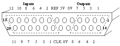
Figure 1, D25 interface connector
Inputs
The 12 ADC input channels
have an input voltage range of 0 to +5V and a resolution of 8bits
(0 to 255), hence 1LSB represents a voltage change of 19.6mV (5V/255).
The inputs should be driven by a source impedance of less than 10KW to prevent errors due to
input currents. Unused inputs should be connected to 0V.
The lower 4 channels connect
directly to the GPI ADC while the upper 8bits are fed via multiplexer. For this
reason inputs 0 to 3 are preferred for high speed/high impedance measurements.
Outputs
The 8 DAC output channels
have an output voltage range of 0 to +5V and a resolution of 8bits (0 to 255) hence 1LSB represents a voltage
change of 19.6mV (5V/255). The output load current should be no greater than ±1mA (analogue mode) or ±5mA (digital mode) per
channel.
Digital and analogue modes
use the same hardware but the software emulates a digital output by producing
either 0V (logic 0) or +5V (logic 1).
REF (pin7)
The reference output is
connected to the ADC/DAC reference supply pins and represents the true
full-scale input/output levels (~5V).
Use this pin to power low current devices (<5mA) eg: potentiometers,
thermistors etc. This pin should not be used as a power supply pin.
5V (pin6)
The 5V supply pin is
connected to the GameBoy power converter and can be used to power external
circuits such as switches, Infrared sensors and real time clocks. The current drawn from this pin should be no
greater than 20mA.
CLK (pin19)
The clock output pin
produces a ~1MHz (976uS) logic signal that can be used to with external
circuits such as counters. The clock is
actually derived from the GameBoy clock and is buffered to drive loads of less
than 5mA.
3.0 Standard Software
Commands
The standard GBGPI software
commands are located in \lib\GPI.H and \include\GPI.S, more advanced (specific)
commands can be added to \lib\GPIA.H and \include\GPIA.S (see section 6.0).
To add the standard command
set to your C applications simply add the following statement to the include
list: #include <gpi.h>. An example program can be found in section 5.0.
read_adc(channel)
Read input channel
and return analogue value.
Channel is 0 to 11, value is 0 to 255.
write_dac(channel, data);
Write to output channel
with analogue value. Channel is
0 to 11, value is 0 to 255.
reset_gpi();
Resets GPI internal hardware
and sets all outputs to zero.
set_bit(channel);
Set output channel to
logic 1 (analogue 255). Channel is 0 to
11.
clear_bit(channel);
Clear output channel
to logic 0 (analogue 0). Channel is 0
to 11.
test_bit(channel,
threshold);
Read input channel
and return logic state. Threshold defines the input voltage level
required to produce a logic 1. Channel
is 0 to 11, threshold is 0 to 255, state is 0 or 1. The threshold value should be set to 40 (0.8V) for TTL/HCT logic
or 128 (2.5V) for CMOS/HC logic.
|
|
All settings |
ADC channel 0-3 |
ADC channel 4-11 |
|
read_adc() |
|
100uS |
200uS |
|
write_dac() |
325uS |
|
|
|
reset_gpi() |
2.5mS |
|
|
|
set_bit() |
350uS |
|
|
|
clear_bit() |
350uS |
|
|
|
test_bit() |
|
120uS |
220uS |
Figure 2, Standard Command Execution Times
4.0 Flash Memory
Selection of the internal flash memory bank is controlled by a combination of hardware logic and a mechanical slide switch. Physically the flash memory is contained within a single device but the functions of the three memory banks are different,
|
Bank |
Size |
Switch position |
GB memory map |
Function |
|
0 |
32KB |
N |
0000 to 7FFF |
32K User Program Store |
|
1 |
1KB |
N |
B000 to BFFF |
4K User Data Store |
|
2 |
32KB |
P |
0000 to 7FFF |
Boot loader for
reprogramming |
Figure 3, Flash Memory Banks
Bank 0, User Program Store
The 32KB program store
contains the compiled ROM image of your application program. Memory locations
0000 to 014F are reserved (by the compiler) to tell the Gameboy what type of
cartridge has been installed etc. This
reserved memory also holds the scrolling NINTENDO logo which appears on
startup, this cannot be changed! The rest of bank 0 is free for development and
should accommodate approximately 700 to 1000 lines of ‘C’ code.
Bank 1, User Data Store
The 4KB non-volatile
programmable data store allows user-defined data parameters to be stored and
retrieved even after the power has been switched off. This is ideal for storing configuration or calibration data that
cannot be defined when the program is written.
A set of special programming commands are provided to enable the user
program to write and read from the data store,
|
Command |
Execution Time |
Function |
|
in_byte(aaaa) |
35uS (RAM) 20mS (video) 35uS (data store) |
Read a single byte from
any memory location |
|
r=out_byte(aaaa) |
35uS (RAM) 20mS (video) 1mS (data store) |
Write a single byte to any
memory location (not ROM) |
|
r=read_store(*b,s) |
s*3mS |
Read (s*256) bytes from
data store into array |
|
r=write_store(*b,s) |
s*256mS typ. |
Write (s*256) bytes from
array into data store |
|
r=erase_store() |
1sec typ. |
Erase all of the data
store (set to 0xFF) |
aaaa = Absolute memory address (0x000 to 0xFFFF).
*b = Pointer to array of (s*256) bytes.
s = Size of data store used * 256 bytes (1 to 16).
r = return result,
0=OK, 1=error.
Figure 4, Bank1 programming commands
The flash data store works
like an EPROM in that you must first erase store setting all of the bytes to
0xFF. It is then possible to program individual bytes by setting the data bits
from 1 to 0, it is not possible to set a bit back to 1 without erasing all
of the store.
From figure 4 it is seen
that there are two ways of writing to the data store, with the out_byte or the
write_store commands the, choice of these commands will depend on your final
application. The following examples illustrate this.
1. If the application was a data logger
then the program would start by erasing the data store. As each byte was logged
it would be programmed into the data store using the out_byte command. At the end of the run all the bytes would be
read from the store before the program could restart.
2. If the application was a temperature
controller then the program would have to randomly update and save set-point
and calibration values. The only way of
achieving this is to have a mirror of the data store in RAM (using an array),
if a value is updated in the array a copy of the entire array would be made in
the data store using the write_store command.
At the start of the program the array would be initialised from the data
store using the read_store command.
The write_store
command actually performs an erase, 256*s byte write, then checks the data was
written correctly, this can be performed over 100,000 times. If you do not wish to use all of the data
store (s=16) then s can be reduced, this has the advantage of using less RAM
memory which is limited to 8K.
Bank 2, Boot Loader Program
Set the manual switch to ‘P’
before switching on the GB to enable the boot loader program. The programming boot loader menu will appear
which allows programming of Banks 0/1 and reading of Bank 1 via the Game Link
port to a PC. The PC software is
windows 95/8 compatible and will download a 32KB image in about 30seconds. Note: software protection will prevent games
ROM’s from being loaded so development ROM’s must have the licensee code (0x014B) set to zero before compiling.
5.0 Example Program
/* GPI demo to read input channel 0 and
output 0 to 255 to channel 0 */
#include <gb.h>
#include <stdio.h>
#include <gpi.h> /* standard GPI library */
void main()
{
UBYTE din, dout;
reset_gpi(); /*
reset GPI hardware */
cls();
printf("GPI Demo\n\n");
printf("GPI IP0=\n");
printf("GPI OP0=");
do
{
gotoxy(8,2);
din=read_adc(0); /*
read input channel 0 */
printn(din, 10, UNSIGNED); /*
display in decimal */
puts(" ");
write_dac(0, dout); /*
output value */
gotoxy(8,3);
printn(dout, 10, UNSIGNED);
puts(" ");
dout++; /*
dout=dout+1 */
delay(100);
}while(!0); /* do forever */
}
To try this program out
simply cut and past it into a new document within your text editor/compiler
(e.g. GBDS). Save it to a suitable
directory e.g. C:\SDK\GBZ80-GB\2-1-0\DEMO\DEMO.C. Then compile and run it. If you get a message like ‘undefined GLOBAL
reset_gpi()’ you have probably not installed the standard GBGPI library
properly, see section 6.0.
6.0 Software
installation
Before adding the GBGPI
library’s you must have completed the following software installation step,
1) Unzip GBDK onto
your hard drive, which should look something like this,
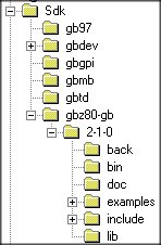
Note:
subdirectories have been added for \gb97 (emulator), \gbdev (development
studio), \gbtd (tile designer), gbmb (map builder), gbgpi (programmer).
2) Make all the GBDK
libraries by running \lib\MAKE.BAT and \examples\MAKE.BAT.
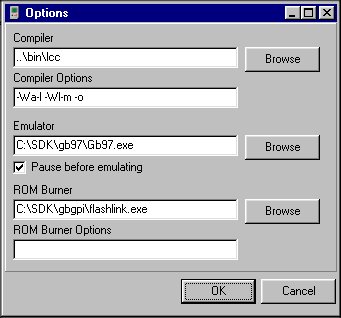
3) If you are using
the GB development studio then set the ‘code editor’ ‘options’ like this,
6.1 Adding GPI
Library Files
To add the standard GBGPI
library commands to GBDK the following files must loaded.
\include\GPI.H - parameter definition for commands
\lib\GPI.S - source code for commands
\lib\GPI.O - output file from GPI.S
\lib\GPIA.S - source code for advanced
commands
\lib\GPIA.O - output file from GPIA.S
\lib\MAKEGPI.BAT - make file for GPI.S and GPIA.S
It is also necessary to add
a reference to GPI.O/GPIA.O in \lib\GB.LIB (add two lines to the end of the
file GPI.O and GPIA.O).
To simplify this process
just unzip GBGPI.ZIP into a within your GBDK path e.g. C:\SDK\GBGPI\ and run
SETUP.BAT. If you get and error during
this process then you have not put the directory in the correct place or you
have not installed GBDK correctly.
6.2 Advanced
Library Files - GPIA
This section is under
development.